Our Unique Plating Technology
Precision Plating for TSV and TGV Applications
Our plating technology for via filling in wafers and glass is used to enable 3D semiconductor packaging, miniaturization, higher density, energy efficiency, high-speed communication, and improved frequency characteristics.
At Kiyokawa, we can embed metal through plating in both blind vias and through vias. This process provides high conductivity, low resistance, excellent thermal conductivity, and efficient wiring formation.
| Electrolytic Copper | High-frequency characteristics, High-density, Miniaturization, Reduced power consumption |
|---|---|
| Electrolytic Nickel | High-density, Miniaturization |
* Please feel free to contact us about specifications not listed above.
Through-Silicon Vias (TSV) and Through-Glass Vias (TGV) are used to connect chips in 3D packaging, enabling enhanced performance through integration.
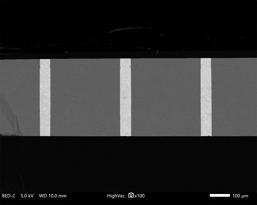
We offer plating services for the vias inside these structures. With our proprietary via-filling plating process, we can achieve void-free, completely filled vias. In addition to silicon and glass wafers, we can also plate through vias on ceramic and resin substrates.
Traditional plating methods required the removal of the plated layers on both sides of the wafer through CMP polishing after plating the vias. However, by using our proprietary plating method, we can reduce the amount of plating on both sides of the wafer, significantly shortening the CMP polishing process.
|
Traditional Method: CMP polishing required on both sides of the wafer. 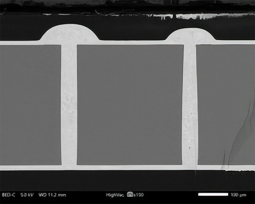
|
(Current) Completed with CMP polishing of the wafer surface only! 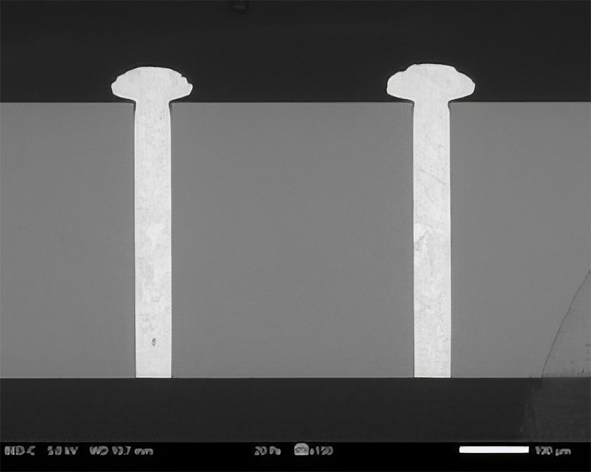
|
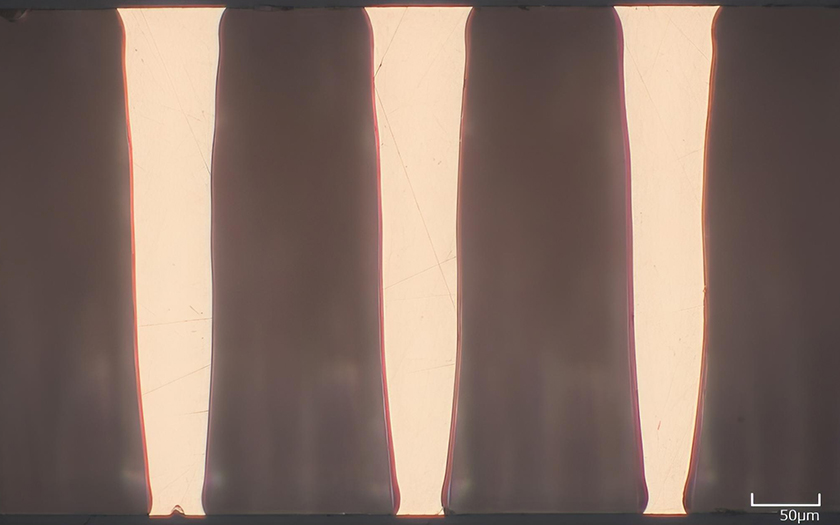
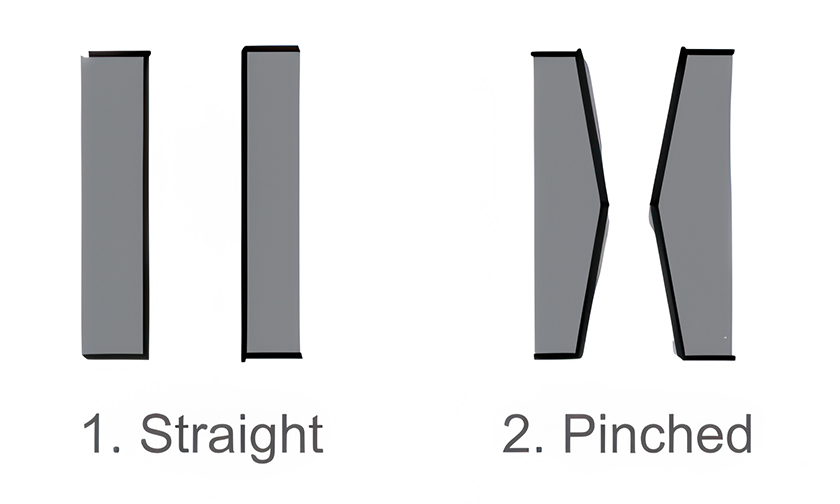
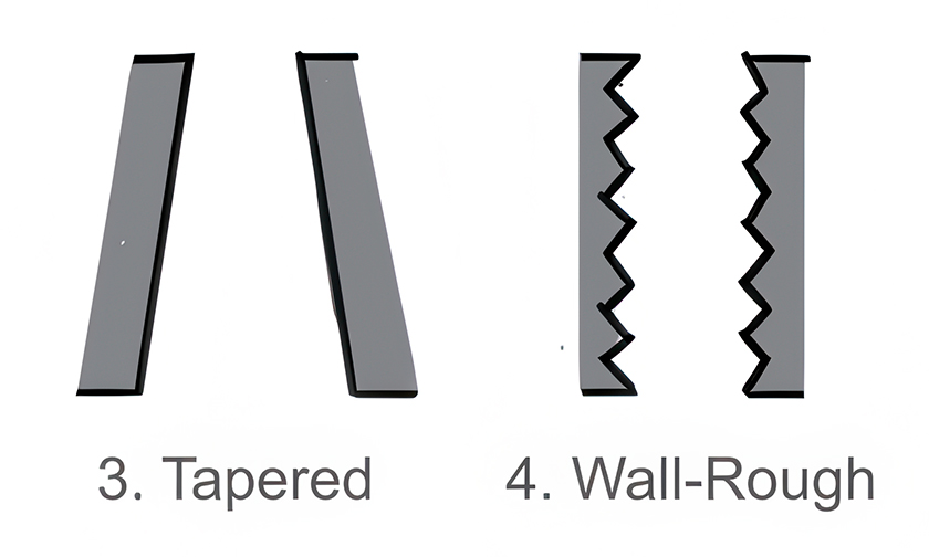
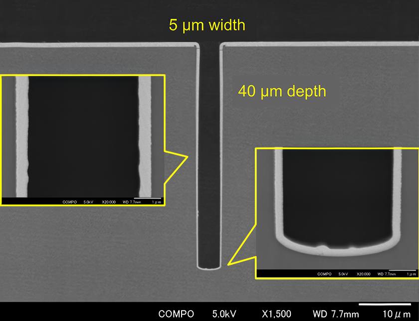
Depending on the method used to form through vias, different via shapes can be created. The plating quality may vary depending on the via shape. We support a variety of via shapes, including straight, necked, tapered, and wall-uneven shapes. Please consult us regarding the choice of metal.
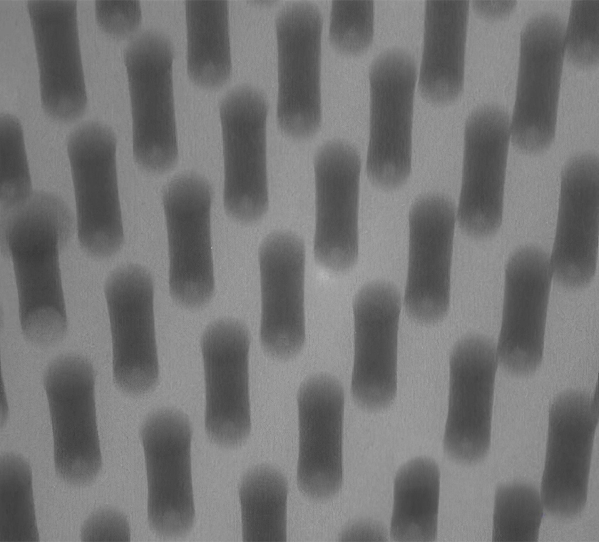
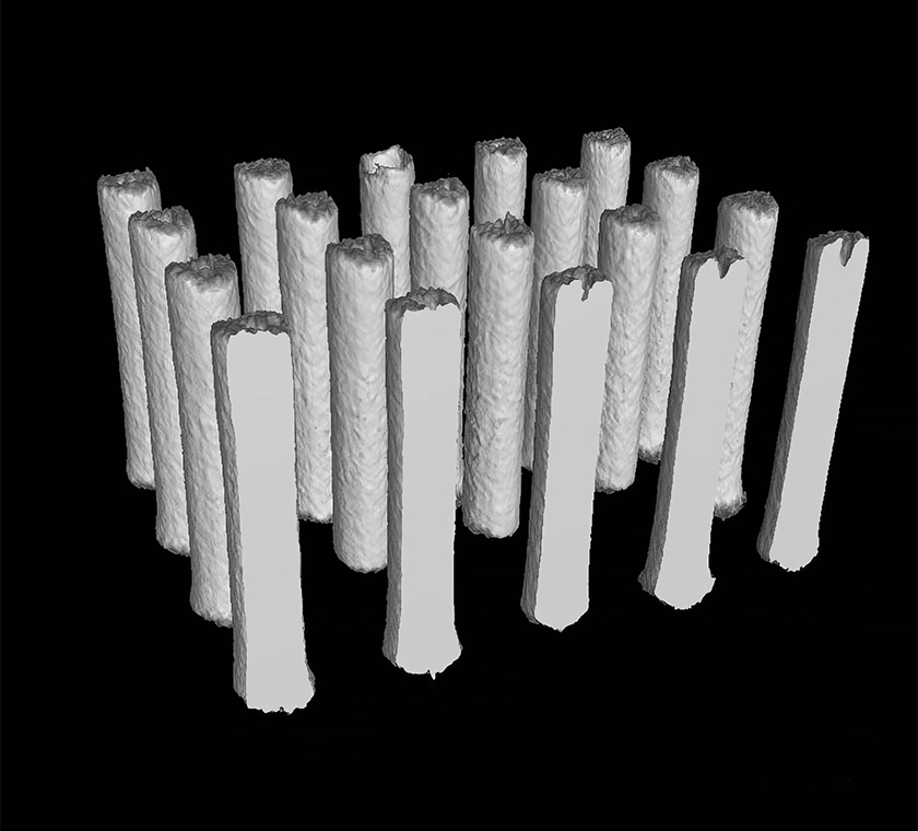
Our non-destructive analysis technology contributes to improved reliability, reduced evaluation time, and minimized sample volume. Using X-ray CT equipment, we can non-destructively to inspect the via filling status inside the vias.
The sample sizes range from chip size up to a maximum of 300 mm square. We also offer evaluations using other methods such as laser microscopy and cross-sectional analysis.
|
|
If you don’t need full via filling but simply require reliable conductivity, consider our conformal plating technology. Conformal plating ensures even coverage on via sidewalls and bottom surfaces, areas that can't be addressed by sputtering. Compared to via-filling plating, this method also leads to reduced plating time.
Can you handle square-shaped substrates?
We may be able to accommodate this. Please contact us for more details.
What sizes have you successfully plated for via-filling?
Our experience shows that we can plate vias with diameters ranging from approximately 30 to 50 μm, and wafer thicknesses of around 200 to 300 μm. Results can vary based on the via shape, so we will evaluate the conditions using actual samples.
Is via-filling possible not only for through vias but also for blind vias?
Blind vias are much more challenging for via-filling compared to conformal plating. Depending on the via dimensions in your substrate, it may be possible to determine feasibility through evaluation. Please reach out to us via the inquiry form below to discuss your requirements.