Our Unique Plating Technology
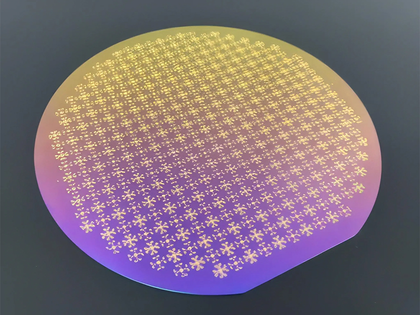
Plating micro bumps and fine wiring is essential for miniaturization and enhanced functionality in semiconductor packaging. With over 20 years of experience in semiconductor wafer plating technology, we contribute to solving customer challenges and realizing products. We support small-scale prototypes and testing projects, starting from a single piece, and are also available for mass production inquiries.
| Electrolytic Copper (Cu) | Wiring, rewiring (RDL), hybrid bonding, Cu sintering bonding, low resistance, heat dissipation |
|---|---|
| Electrolytic Nickel (Ni) | Barrier metal (diffusion prevention) |
| Electrolytic Gold (Au) | Solder bonding, wire bonding, Au-Au bonding, ACF bonding, oxidation resistance, low resistance |
| Electrolytic Tin-Silver (SnAg) Alloy | Lead-free bonding |
| Electrolytic Gold-Tin (AuSn) Alloy | High-temperature bonding |
| Electrolytic Rhodium (Rh) | Surface hardness, wear resistance |
| Electrolytic Indium (In) | Low-temperature bonding |
* Please feel free to contact us about specifications not listed above.
We offer tailored bump, wiring, and pad plating technologies to meet your product design, application, and challenge needs. Contact us for more details.
|
|
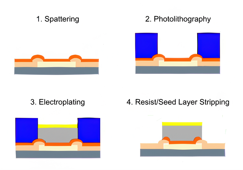
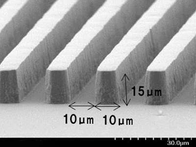
In addition to plating for bump and wiring formation, we provide a full range of processes, including seed layer formation through sputtering, resist patterning via exposure/development, and the removal of resist and seed layers. Our advanced equipment and technology allow us to deliver these processes as a complete solution, helping reduce your design timeline.
*Note: Our selective etching minimizes side-etching.
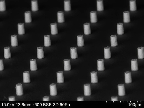
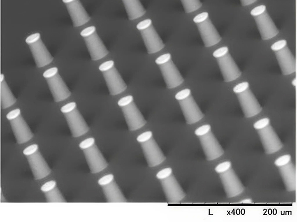
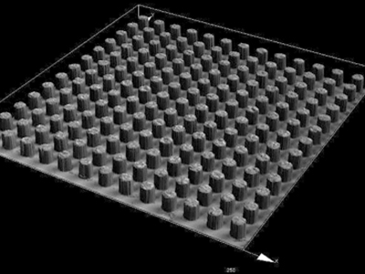
Our integrated process allows for the formation of microbumps and fine-line wiring.
For plating-only processes, we have experience in even finer and smaller patterns.
*Please consult with us as the capabilities may vary depending on plating thickness and shape.
*For detailed specifications, please refer to the downloadable materials.
|
|
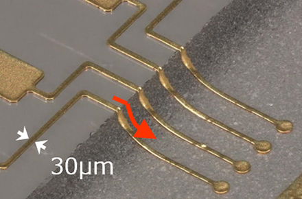
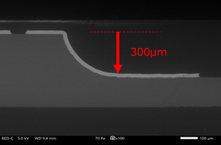
Even for substrates with height variations, which are necessary for 3D and high-density mounting, we offer wiring plating that conforms to the substrate’s contours.
・Wiring width can be reduced to as small as 30μm
・Wiring formation is possible even for steep slopes up to 300μm in depth
*Note: Please consult with us as the response may vary depending on the slope and shape of the substrate.
|
|
Can you handle not only round shapes like wafers but also split or chip shapes?
Depending on the shape, we may be able to accommodate your request. Please contact us for more details.
Can you process plating types or specifications not listed above?
We may be able to accommodate your request depending on the specifics. Please contact us for more details. Please note that additional time may be required for preparation.
Is it possible to handle substrates with thin thicknesses?
It depends on the material, but we have experience working with thicknesses around 100μm.
Can you perform partial processes like sputtering only, photolithography only, or stripping only, in addition to plating?
Yes, we can accommodate those requests. However, some specific requirements may not be possible, so please contact us for further details.
How is the exposure mask for photolithography created?
We will arrange the creation of the mask based on the drawing data you provide. Please provide the drawing in either DXF or DWG format.