Proven Mass Production
Under-Barrier Metallization by Electroless Plating for Power Devices
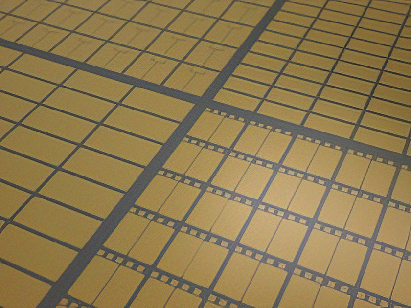
Electroless UBM plating is widely used in the bonding of semiconductors such as Si, SiC, and GaN. Kiyokawa has extensive experience in mass production of power semiconductors for automotive applications, and with our know-how and proprietary technology, we provide customers with stable plating quality. From prototype development to mass production at tens of thousands of pieces per month, including 12-inch large-scale production and electroless thick copper plating for special applications, we cater to a wide range of customer needs.
| Electroless nickel/gold | for solder bonding |
|---|
| Electroless nickel/palladium/gold | heat resistance, thermal diffusion suppression, and wire bonding |
|---|---|
| Electroless copper (thick plating) | copper wire bonding, copper sinter bonding, low resistance, high current, and heat dissipation applications |
| Electroless low-phosphorus nickel/gold | high-temperature resistant nickel coating |
| Electroless nickel/gold (thick plating) | solder bonding and corrosion resistance |
* Please feel free to contact us about specifications not listed above.
We provide electroless nickel-phosphorus/gold plating for aluminum electrodes on semiconductor wafers, with years of proven success in mass production for automotive power semiconductors.
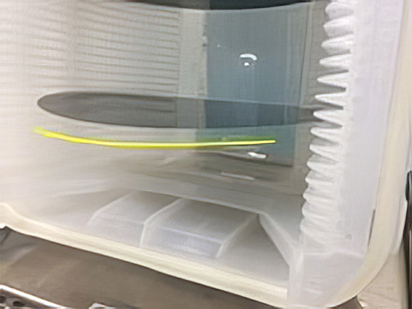
In recent years, wafer thinning has progressed to improve product performance. However, in plating processes, as the wafer thickness decreases, issues such as wafer warping or bending arise.
These problems can lead to wafer contact or damage during processing multiple wafers at once in the plating cassette, as well as affect the uniformity of the plating thickness. Kiyokawa has developed a unique plating cassette that solves these challenges, enabling the plating of ultra-thin wafers as thin as 60μm.
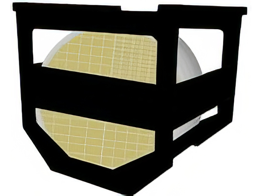
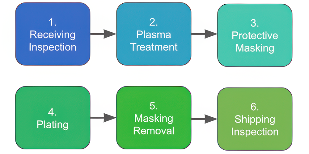
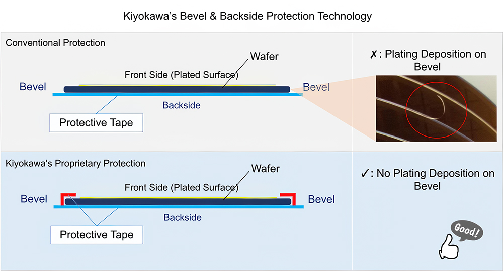
The electroless UBM plating process uses chemical reactions, so if proper masking (protection) is not applied to the correct areas, plating can deposit on unintended electrodes, affecting the quality.
For example, if plating is deposited on the back or bevel areas without proper protection:
To address these challenges, Kiyokawa offers a unique protection technology that not only protects the back but also protects the bevel surface. This ensures plating deposition on both the back and bevel surfaces is completely prevented.
The following options are available, so please feel free to contact us for further details:
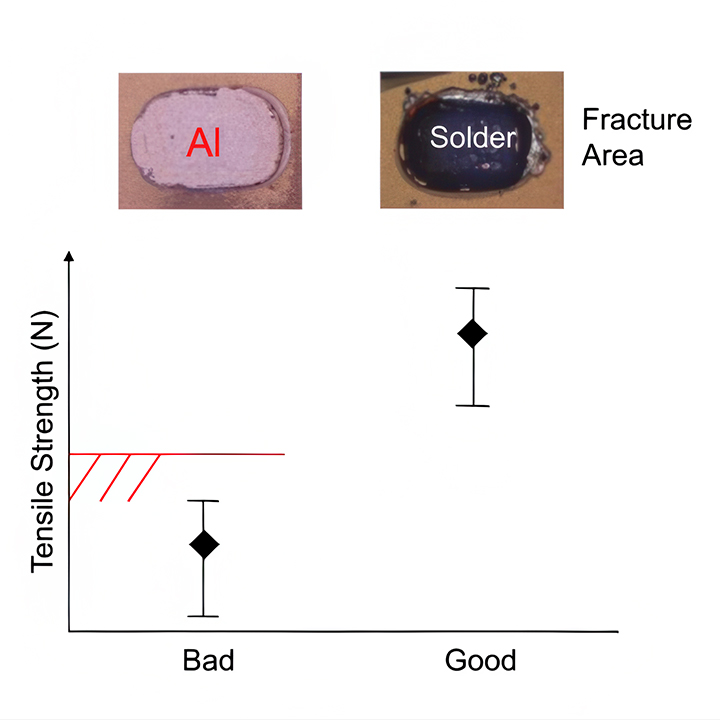
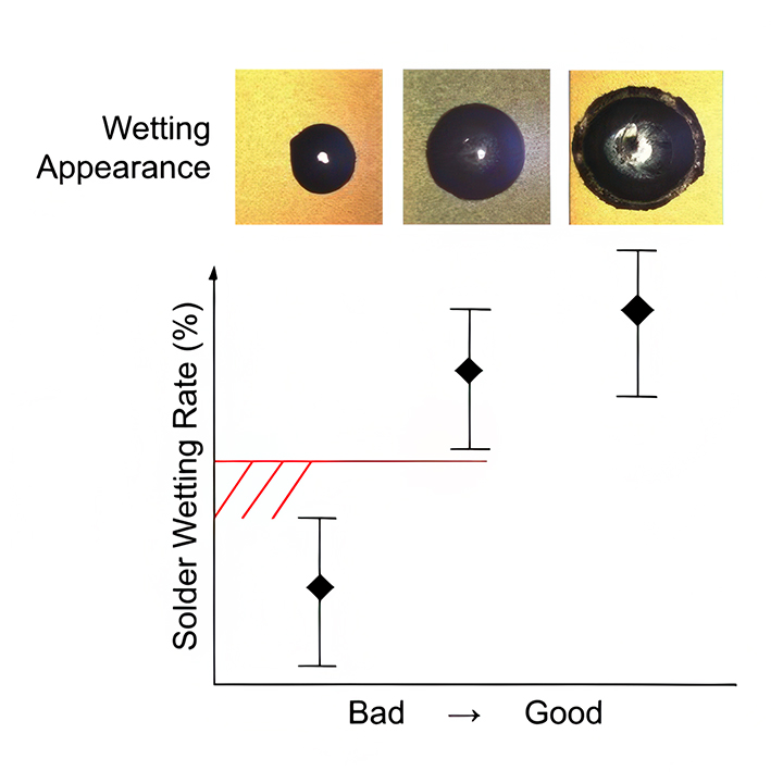
Electroless UBM plating films are used in various bonding applications such as solder joints, wire bonding, and sintering joints. Specifically, adhesion strength and solder wetting properties are crucial evaluation criteria for these joints.
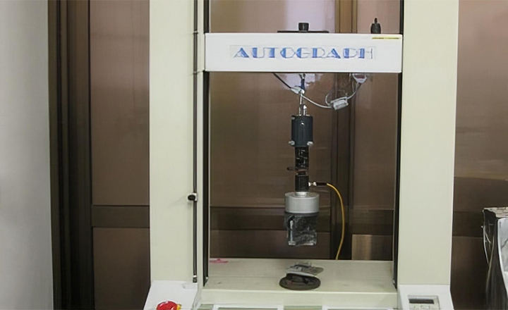
For adhesion strength evaluation, while simple methods like tape tests are available, when numerical comparison is required, we can perform plating adhesion strength evaluations using our proprietary methods.
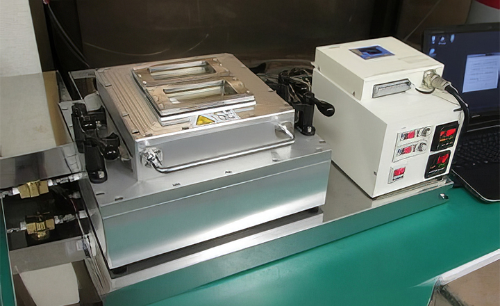
Reflow in a hydrogen-reduced atmosphere, and measure the solder spread area to properly evaluate the solder wetting properties.
| Adhesion Strength Evaluation | Solder Wetting Evaluation | |
|---|---|---|
| Objective | To evaluate the adhesion strength between the base Al electrode and the Ni plating layer. | I would like to evaluate the solder wetting properties of the gold-plated coating quantitatively. |
| Test Device |
|
|
| Evaluation Example |
|
|
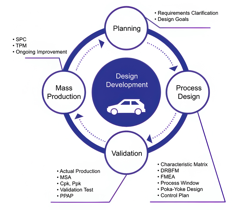
Semiconductor plating requires precise and reliable quality due to the delicate and intricate nature of the products, and even higher standards are required for automotive applications.
With over 20 years of experience in semiconductor plating development and a solid design and development process, we effectively control quality risks and lead the process to mass production. Additionally, with a wide range of automated plating lines for mass production, we are able to evaluate from prototype to production-scale equipment, ensuring smooth development while minimizing any changes during the equipment transition phase.
These thorough quality designs have resulted in zero market complaints over 10 years of automotive mass production. We ensure stable quality mass production tailored to our customers' requirements.
We offer electroless thick copper plating tailored for high-current applications, such as SiC power semiconductors. Thick copper plating is effective for copper-to-copper bonding, such as copper wire bonding, copper ribbons, and copper sintering, as well as additional wiring substrates, thanks to its low resistance and heat dissipation properties.
In addition to electroless Ni/copper plating on Al electrodes, we can also propose our proprietary technology for direct electroless thick copper plating on Al electrodes. We are able to create prototypes with copper film thicknesses tailored to your specifications, so please feel free to reach out to us.
What type of coating is needed for areas where plating is not desired?
For the backside and bevel areas, our protective technology prevents plating deposition. However, for protecting device surfaces, we recommend using insulating films with chemical resistance, such as polyimide or SiO2.
What is the maximum thickness for electroless Ni/Au plating?
Ni plating can be applied up to a thickness of about 10-20μm. However, as the Ni film thickness increases, there is a tendency for the wafer (substrate) to warp due to increased stress.<br>Au plating typically has a thickness of about 0.04μm, but if a thicker coating is required, it can be plated up to approximately 1μm using a thick-plating process.
Is it possible to perform plating using electroplating in addition to electroless plating?
We also offer electroplating processes. By combining these with our photolithography processes, various electroplating options can be applied on the electrodes.
Is it possible to plate chip-sized wafer fragments or small-diameter wafers?
Using specialized protective technology and plating fixtures, plating treatment is possible for such cases (subject to consultation).