
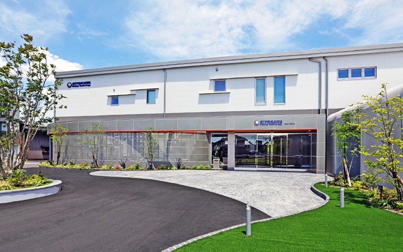
Empowering Next-Generation Semiconductorswith Advanced Plating.
Equipment used by Kiyokawa Plating Industries Co, Ltd.
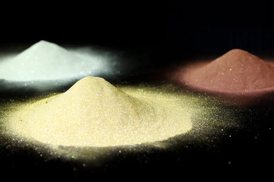
Revolutionizing Powder Materialswith Nano Plating Technology.
Examples of materials used by Kiyokawa Plating Industries Co, Ltd.
Plating Quality Made in Japan, Trusted Worldwide.
Staff of Kiyokawa Plating Industries Co, Ltd.
 

Our Services

  • Electrolytic UBM Plating: Bumps & Lines

    Optimize your semiconductor designs with our high-precision solder bump electroplating and micro-wiring solutions for wafer applications.

  • TSV & TGV Via Plating

    Discover our advanced via filling plating technology for wafers and glass, perfect for 3D packaging, miniaturization, and high-density integration.

  • Electroless UBM Plating for Power Devices

    Find reliable electroless UBM plating solutions for semiconductor bonding, ideal for automotive, power devices, and high-performance applications.

  • Plating on Powdered Materials

    Enhance your materials with advanced powder plating for better conductivity, corrosion resistance, and electromagnetic shielding.


Explore More Plating Solutions

Our Japanese website features a wide range of advanced plating technologies and application examples for
Medical Devices, Electronic Components, Substrates, Magnets, and other specialized industries.
Most modern browsers can automatically translate these pages into your preferred language.

Quality Assurance

At Kiyokawa, we ensure rigorous quality control in plating, leveraging years of experience in mechanical, electronic, semiconductor, and medical parts with advanced nano-level analysis.

About  KIYOKAWA

Learn about Kiyokawa Plating Industries' corporate philosophy, history, and dedication to quality, innovation, and environmental sustainability.


News

SEMICON Taiwan 2026 Exhibition Announcement | September 2–4 | Booth I2900

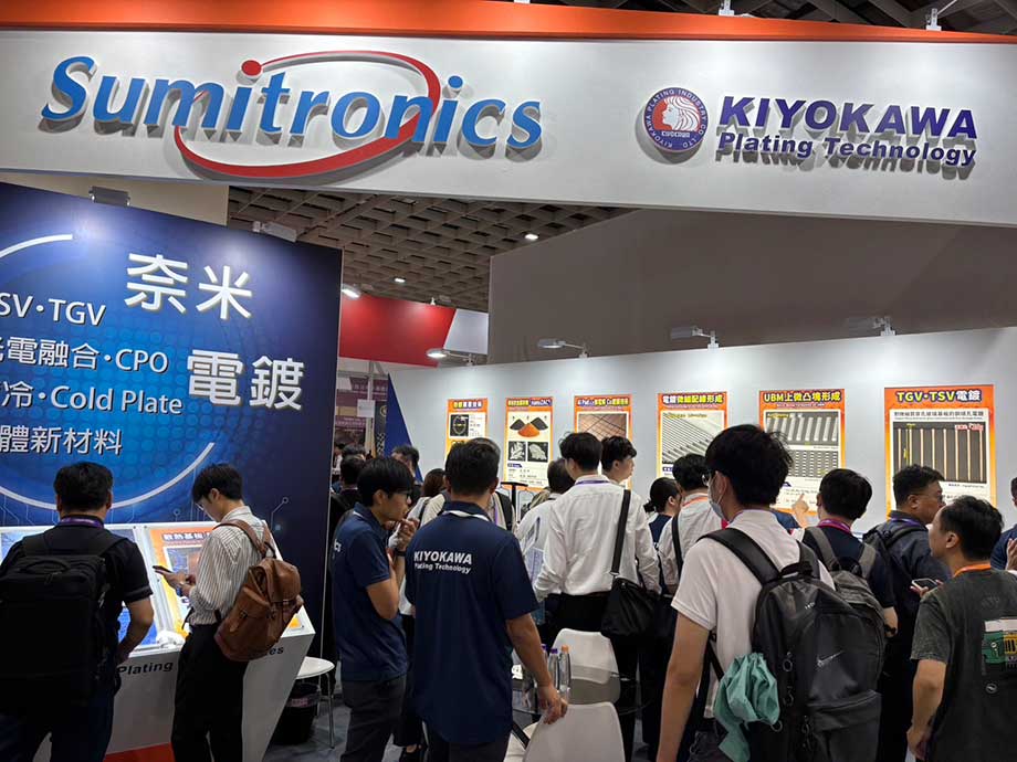
KIYOKAWA PLATING INDUSTRY CO., LTD. is pleased to announce that we will jointly exhibit with Sumitronics Taiwan Co., Ltd. at SEMICON Taiwan 2026, taking place September 2–4.

At our booth, KIYOKAWA will showcase its latest plating technologies under the theme:

Advanced Plating for AI Thermal Management, Semiconductor Packaging & Functional Materials

Featured technologies include:

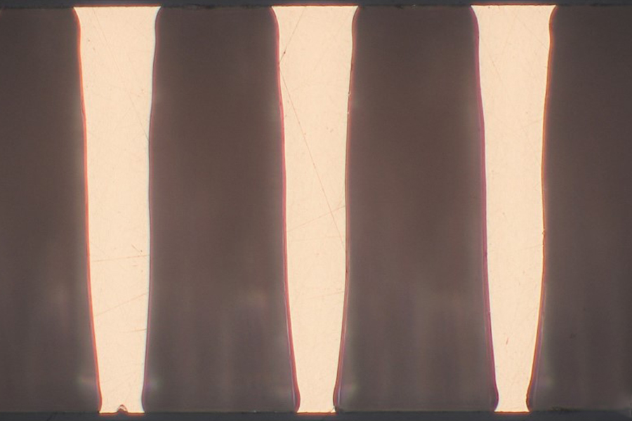
  • Void-Free Cu Filling for TSV/TGV
    For Si, SiC and glass substrates, including high-aspect-ratio vias
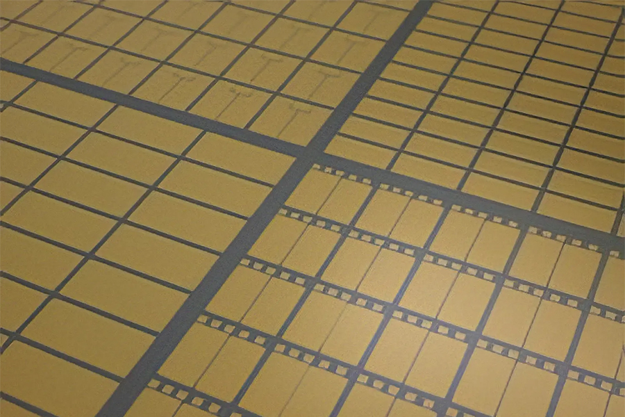
  • Fine Bump, Pillar & RDL Plating
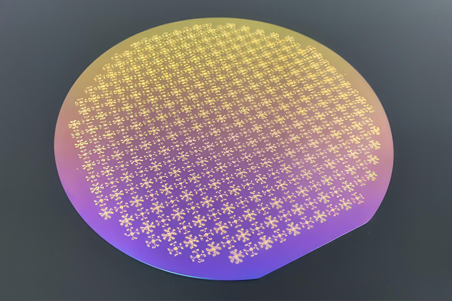
    Integrated processing from seed formation to stripping, up to 12-inch wafers
  • Electroless UBM & Thick Cu Plating
    For bonding, high-current and thermal applications
  • Selective Plating for Thermal Management Components
    For Al and Cu heat-dissipation substrates used in automotive power semiconductors and liquid-cooling components for AI servers
  • Powder Plating for New Material Development
    Creating new functionality by combining various powders with plated metals
  • nanoZAC® Dendritic Metal Powders
    High-purity, high-surface-area and low-density metal powders for conductive and catalytic applications

From a single prototype to mass production, KIYOKAWA provides flexible support for challenging plating requirements.

Have a plating challenge that conventional processes cannot solve? Bring it to us.

SEMICON Taiwan 2026
September 2–4, 2026
Booth I2900

View our SEMICON Taiwan Exhibitor Page

We look forward to welcoming you at our booth.

KIYOKAWA PLATING INDUSTRY CO., LTD. × Sumitronics Taiwan Co., Ltd.

KIYOKAWA PLATING INDUSTRY CO., LTD. × Sumitronics Taiwan Co., Ltd.

Your unique plating solution starts here.